


EdgeLock® Assurance
The NHS52S04, part of the EdgeLock Assurance program, is designed to meet industry standards and follows NXP's security-by-design approach.
The NHS52S04 provides connectivity solutions for medical IoT applications. The NHS52S04 device constitute a highly integrated, single chip, ultra-low-power Bluetooth® Low Energy 5.3 wireless transceiver with embedded microcontroller and flash.
Because of the integrated ultra-low-power radio and flash, the NHS52S04 provides extended battery lifetime. The NHS52S04 is a cost-effective solution within a small solution area required for body-worn sensors and actuator applications like smart skin patches, smart inhalers and vital signs monitoring.
The NHS52S04 runs directly from a Lithium battery or from an external PMIC-based product architecture.
Built with advanced security in mind, the NHS52S04 is part of the NXP EdgeLock® Assurance program.
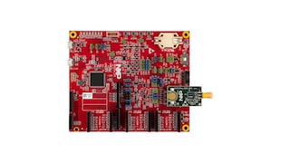
NHS52S04 and enablement (documentation, software and boards) are available for select customers. For additional information and sample availability, contact support or your local sales representative.
Choose a diagram:
| Characteristics | QN908x | NHS52S04 |
|---|---|---|
| Processor | M4F @ 32 MHz | M33F with TrustZone @ 32 MHz |
| Memory | ROM 256 KB | ROM 256 KB |
| RAM 128 KB | RAM 128 KB | |
| NVM 512 KB | NVM 1024 KB | |
| BLE TX | up to +2 dBm | up to +6 dBm |
| BLE RX | N. A. (BLE 125 kbps) | -100 dBm (BLE 125 kbps) |
| N. A. (BLE 500 kbps) | -98 dBm (BLE 500 kbps) | |
| -95 dBm (BLE 1 Mbps) | -95 dBm (BLE 1 Mbps) | |
| -92 dBm (BLE 2 Mbps) | -92 dBm (BLE 2 Mbps) | |
| Interfaces | 35 GPIOs / 4 Flexcomms / SPIFI / USB / ADC / DAC | 23 GPIOs / 3 Flexcomms / SPIFI |
| Security | TRNG, AES-128 | TRNG, AES-256, RSA-4096, ECC P384, SHA-2 |
| Secure Boot, Debug Authentication and Secure GPIOs | ||
| PUF (Physical Unclonable Function) | ||
| PRINCE (Flash encryption) | ||
| PFR (Protected Flash Regions) | ||
| Supply Range | 1.8 V ~ 3.6 V | 1.8 V ~ 3.6 V |
| Battery Management | Integrated Buck | Integrated Buck |
| Package | 6 x 6 mm HVQFN48 | 5 x 5 mm HVQFN40 |
| 3.2 x 3.2 mm WLCSP | 2.63 x 2.495 mm WLCSP | |
| Low Power mode | 2.8 µA | 3.0 µA |
| (32-kHz OSC on / 64 KB RAM ) | (32-kHz OSC on / 64 KB RAM ) | |
| Power-off mode | N.A. | 80 nA |
| Radio mA No DCDC |
10.3 mA @ 1.3 V RX @ 2 Mbps 7.1 mA @ 1.3 V TX @ 0 dBm |
6.7 mA @ 1.1 V RX @ 2 Mbps 8.5 mA @ 1.1 V TX @ 0 dBm |
| Radio mA 3 V with Buck |
5.0 mA @ 3 V RX @ 2 Mbps 3.5 mA @ 3 V TX @ 0 dBm |
3.9 mA @ 3 V RX @ 2 Mbps 5.2 mA @ 3 V TX @ 0 dBm |
The NHS52S04, part of the EdgeLock Assurance program, is designed to meet industry standards and follows NXP's security-by-design approach.
1 hardware offering
2 software files
Note: For better experience, software downloads are recommended on desktop.